
Semiconductor

Test and Process Technology for the Semiconductor Industry:

Absolute Precision for the Highest Standards

Effectively Preventing Downtime in the Semiconductor Industry

The semiconductor industry is a field of superlatives: miniaturization, the highest levels of purity, and complex manufacturing processes define everyday operations. In testing and process technology, this means absolute precision, seamless control, and the ability to detect even the smallest deviations. Errors in production are not only costly but can render entire batches unusable. You need systems that not only function technically but also operate reliably, with documented and audit-proof processes in series production while meeting the highest purity requirements.

What Matters in Semiconductor Manufacturing

Cleanroom Compatibility

Equipment and processes must meet the highest purity standards.

Microprecision

Extremely tight tolerances and highly accurate measurements are critical.

Process Stability

Any fluctuation can compromise the quality of sensitive components.

Traceability

Complete documentation of every manufacturing step is essential.

Equipment tailored to semiconductor processes

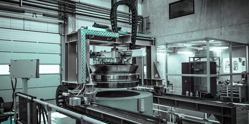
Our testing and processing systems are designed to operate reliably in cleanroom environments and integrate seamlessly into your highly sensitive production lines. Cycle time, test sequences, and process behavior are specifically coordinated to ensure maximum yields.

  • Designed for cleanroom classes up to ISO 5
  • Integration into existing production lines

  • Stable and repeatable processes with microprecision
  • Minimal impact on the production flow

Measurement under cleanroom conditions

Sensitive components are tested under conditions that correspond to their intended use and purity requirements. Pressure profiles, leak rates, and threshold limits are specifically defined to obtain meaningful results that guarantee the integrity of your products.

  • Defined pressure build-up and release profiles for sensitive components
  • Simulation of dynamic loads without contamination
  • Reproducible test conditions under cleanroom conditions

Typical Tasks in the Semiconductor Industry

aprotec_bauteil_wafer-5

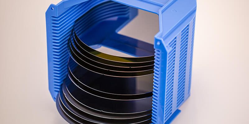
Wafer edges

Edge rounding to prevent chipping and damage.

aprotec_bauteil_wafer-6

Growth crucibles

Oxidation to protect against wear and undesirable material reactions.

aprotec_erfolg_zuechtungsanlagen_heizstab

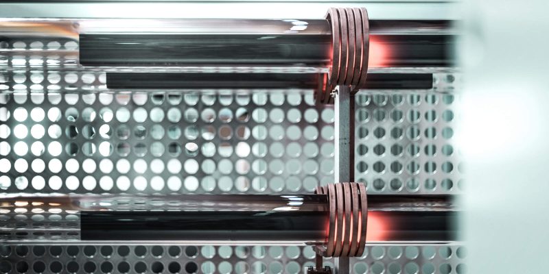
Semiconductor materials (e.g., germanium)

Zone melting for targeted purification and microstructure optimization of the material.

aprotec_bauteil_wafer-1

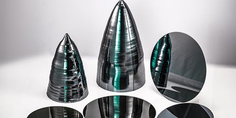
Bulk crystals

Crystal growth (PVT, VGF, etc.) for the production of high-purity single crystals for wafer production.

aprotec_bauteil_wafer-2

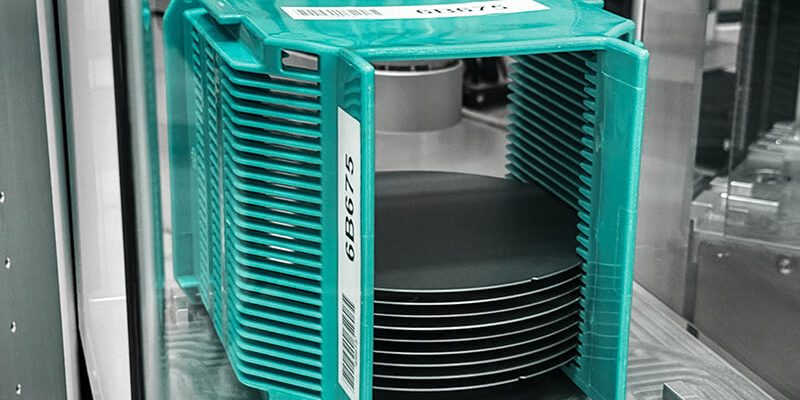
Wafers

Geometry and topography inspection to ensure precise dimensions and flatness.

aprotec_bauteil_wafer-4

Compound semiconductor wafers

Etching process for residue-free surface treatment and cleaning.

This is how we’ve solved it for others​

Find out how companies are using aprotec’s solutions to meet a wide range of industry requirements and make targeted improvements to their processes. The case studies demonstrate how efficiency can be boosted and specific challenges successfully overcomelet them inspire you in your own projects.

Why Aprotec?

Direct contact

You speak directly with the people in charge, not through multiple layers of management

Integrated solutions instead of standalone solutions

Pressure, leak, functional, and measurement tests can be combined in a single system

Experience with a wide range of testing tasks

From simple production line testing to fully automated special applications

Designed for extreme conditions

High pressures, minute leaks, or precise measurement requirements are specifically accommodated

Scalable from single tests to series production

From manual test stations to fully automated systems with cyclic operation
Get Expert Advice

Do you have questions or are you unsure which system is the right fit for your requirements? No problem. We are happy to advise you personally and work with you to find the ideal solution for your application. Benefit from our years of experience, an honest assessment, and professional guidance — tailored to your needs and with no obligation.

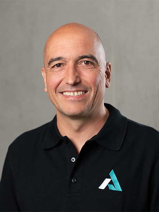
Contact person

Michael Landgraf

Managing Director