
WaferVision HSM-200

WaferVision HSM-200

for High-Precision Wafer Inspection

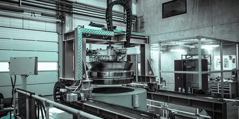
Cleanroom-Compatible High-Speed Measurement System for Wafer Thickness and Surface Topography in the Semiconductor Industry.

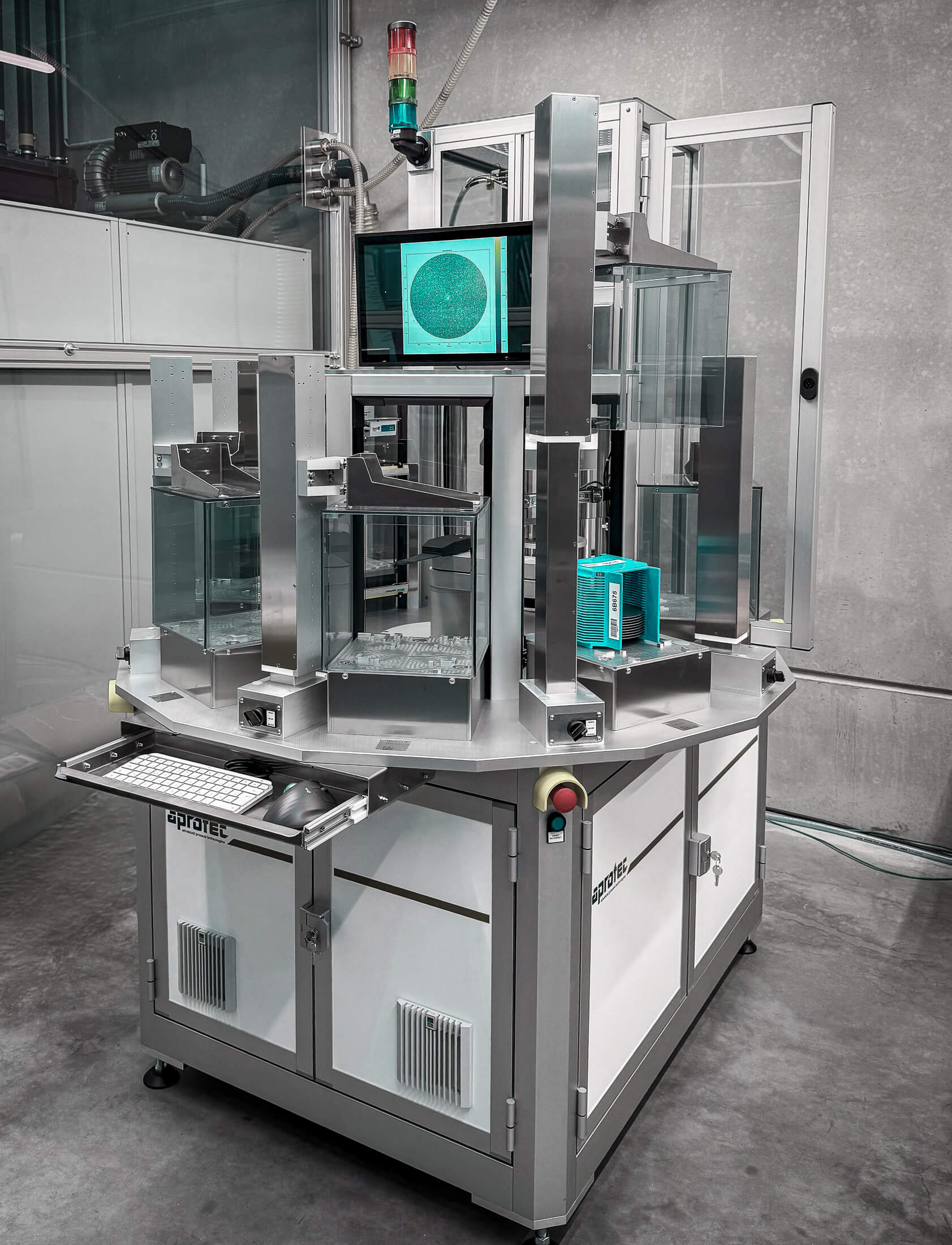
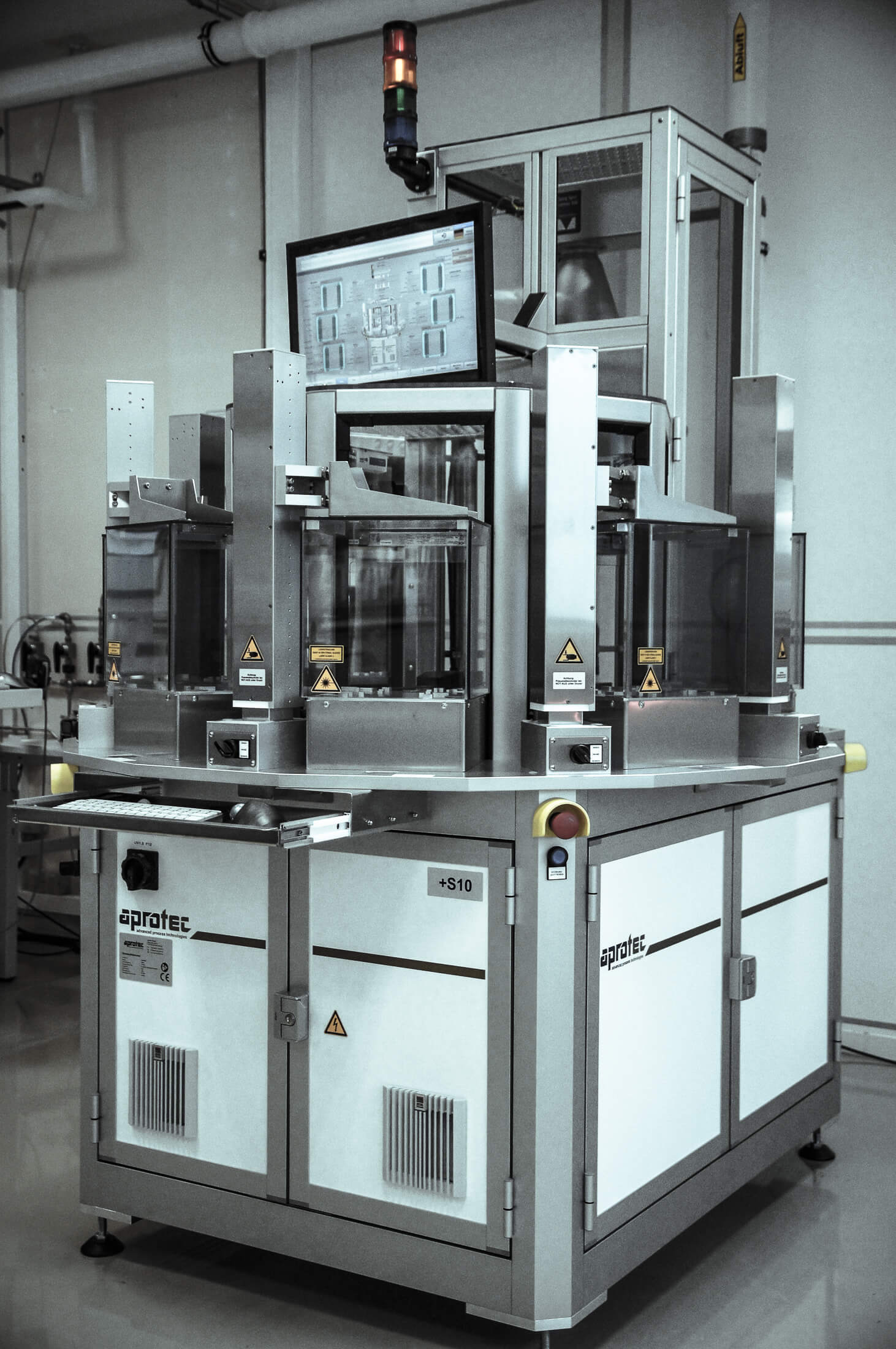
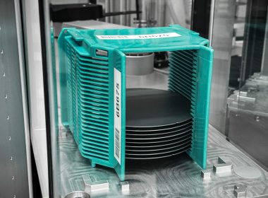
This high-speed measurement system enables precise thickness and surface determination of silicon wafers. It ensures highly homogeneous wafer batches for downstream polishing processes while maintaining an extremely high throughput.

130

Wafer Pro per hour

50 NM

Repeatability Thickness

4‘ to 8’

wafer size

ISo 5

suitable for cleanrooms

The Challenge

Homogeneous Wafer Batches for Optimal Polishing Results

To achieve optimal, uniform polishing runs in semiconductor manufacturing, the wafers used must feature an exceptionally homogeneous thickness distribution. The customer faced the challenge of precisely sorting and classifying high volumes of wafers prior to polishing to prevent uneven processing and costly scrap.

At the same time, the modern production environment demanded seamless software integration with the factory host system and strict compliance with cleanroom standards, all without sacrificing measurement speed.

The Requirement: A fully automated, cleanroom-compatible inspection system that captures wafer thickness and surface topography with sub-micrometer accuracy, communicates with existing manufacturing execution systems, and guarantees high throughput.

The Solution

Sub-Micrometer Precision at High Speed

The WaferVision HSM-200 provides a highly innovative measurement solution that inspects up to 130 wafers per hour with a thickness repeatability of 50 nm. Certified for ISO Class 5 cleanroom environments, the system features a SECS/GEM interface, making it fully ready for smart factory integration.

Measurement Method

Wafer thickness and surface topography measurement

Measurement accuracy: topography

Compressed air (preliminary test) · Helium (precision leak detection)

Throughput

130 wafers per hour

Supported Component Types

Wafer sizes from 4" to 8"

Measurement accuracy: thickness

0.1 micrometre accuracy

Integration & Software

SECS/GEM ready for automated factory communication

Thickness Repeatability

50 NM

Cleanroom Class

Cleanroom compatible per ISO Class 3
Test methods used

These processes have been combined for this plant and can also be used individually, depending on requirements.

aprotec_erfolg_WaferVision HSM-200-5

Wafer inspection

to record geometric properties and ensure quality throughout the entire manufacturing process.

Typical applications:

  • Wafer qualification
  • Process monitoring during semiconductor manufacturing
  • Final inspection
  • of silicon, compound semiconductor and other flat substrates
  • for measuring parameters such as thickness, warp, bow and TTV

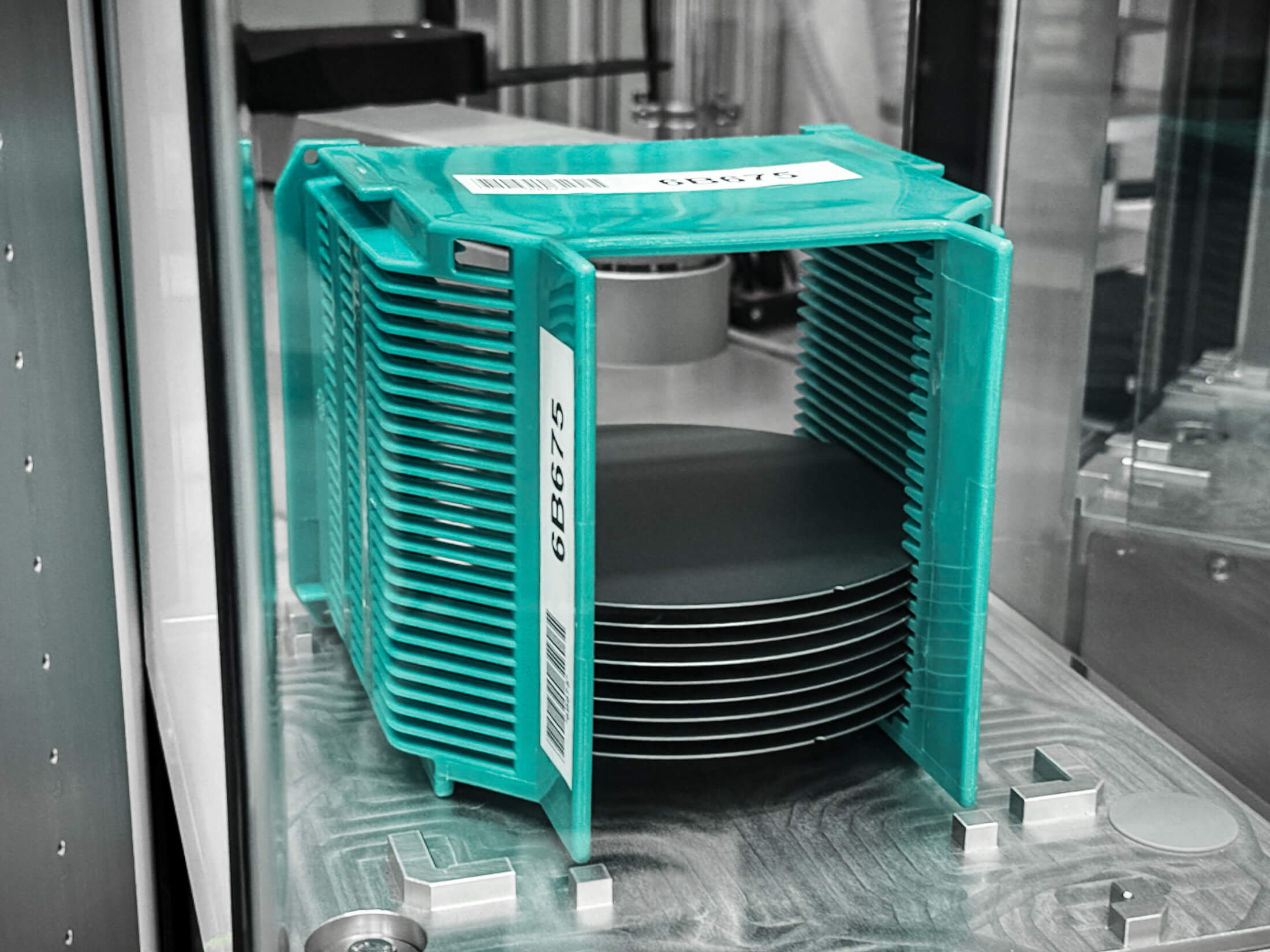
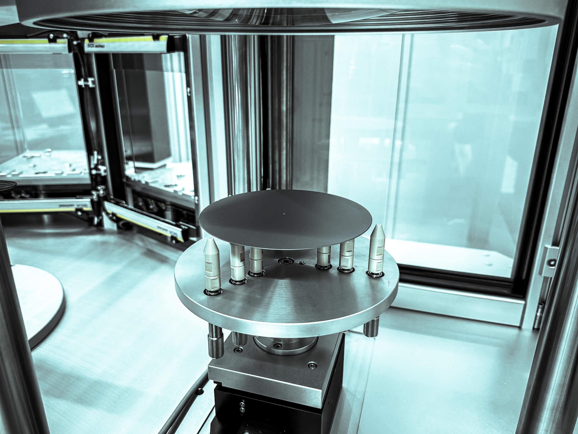
System Gallery

Insights into the System

More Systems

Discover how companies use aprotec solutions to master diverse industry requirements and purposefully enhance their processes. These real-world examples demonstrate how efficiency is increased and individual challenges are successfully resolved. Get inspired for your own projects.

Get Expert Advice

Do you have questions or are you unsure which system is the right fit for your requirements? No problem. We are happy to advise you personally and work with you to find the ideal solution for your application. Benefit from our years of experience, an honest assessment, and professional guidance — tailored to your needs and with no obligation.

Contact person

Michael Landgraf

Managing Director