Wafer Testing

Wafer Testing

for Semiconductor Quality Assurance

Custom wafer measurement systems for qualifying semiconductors throughout the entire manufacturing process.

Surface Defects as a Quality Risk

In wafer manufacturing, even the smallest defects pose a threat to the functionality and quality of the wafers. Microcracks, scratches, or stresses arise during processing and are often invisible. Without precise early detection, failures in semiconductor manufacturing are virtually unavoidable. A defined quality standard therefore requires precise inspection methods to ensure the integrity of high-quality wafers.

aprotec_content_wafer

Wafer Inspection Precisely Tailored to All Requirements

Our inspection systems are precisely tailored to the wafer’s geometry and thickness, in order to detect surface defects, material deviations, deformations, and process variations at an early stage. We define measurement strategies, scan parameters, and evaluation algorithms on a case-by-case basis.

  • Adaptation to wafer geometry
  • Defined measurement profiles
  • Integration into production processes
  • Can be combined with other analysis methods

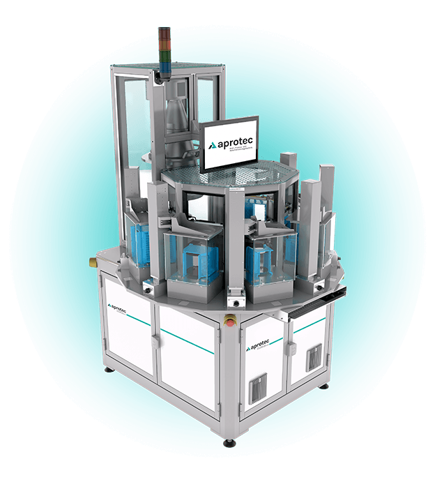
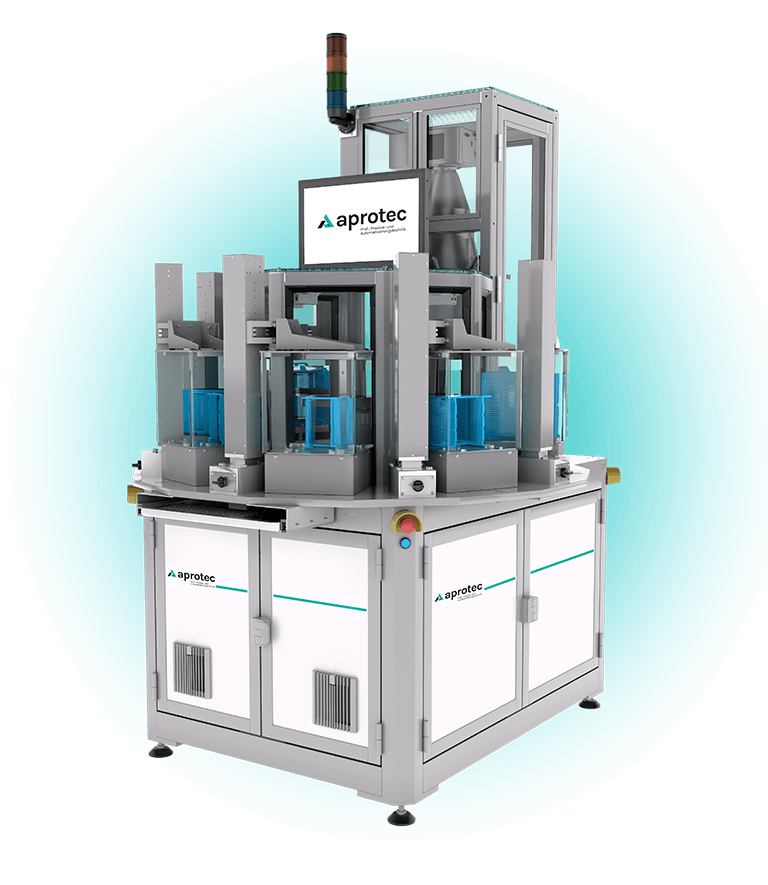
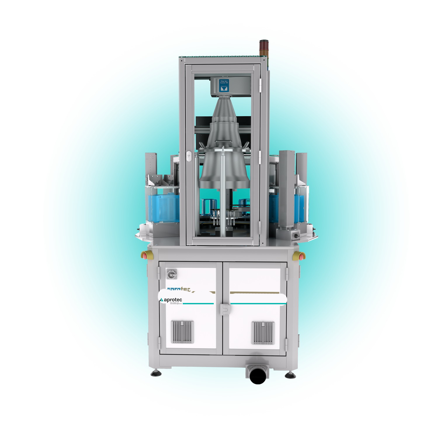
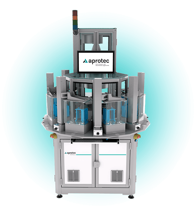
Wafer Measurement System - WaferVision HSM-200

Customizable applications

Sorting, measurement, and qualification for subsequent process steps

Motion-free measurement

Precise and repeatable results without mechanical interference with the test specimen

ISO 3 cleanroom-compatible

Highest cleanliness standards in sensitive production environments

Configurable measurement recipes

Maximum flexibility in adapting to a wide variety of testing requirements

Wafer Inspection Process

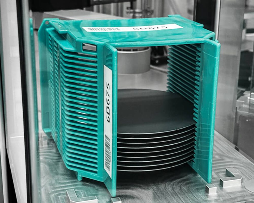
Wafers can be fed into the system manually or automatically and optically measured across their entire surface. Using an interferometric measurement method, wafer thicknesses, surface structures, and topographical deviations are recorded with high precision, using a non-contact, motion-free process. Intelligent evaluation algorithms analyze the acquired measurement data in real time, enabling a reliable assessment of previous processing steps. This allows even the smallest deviations, surface defects, or process variations to be detected early on, enabling targeted optimization of manufacturing processes.
Erfolgsgeschichten rund um Waferprüfung entdecken

Erfahren Sie, wie Unternehmen mit Waferprüfung von aprotec die Qualität ihrer Bauteile sichern und Prozesse zuverlässig validieren. Die Beispiele aus der Praxis zeigen, wie individuelle Anforderungen umgesetzt und Prüfabläufe effizient gestaltet werden – lassen Sie sich davon für Ihre eigenen Projekte inspirieren.

Industry Solutions

We Develop Solutions Tailored to Your Industry

Download our brochure

Get Expert Advice

Do you have questions or are you unsure which system is the right fit for your requirements? No problem. We are happy to advise you personally and work with you to find the ideal solution for your application. Benefit from our years of experience, an honest assessment, and professional guidance — tailored to your needs and with no obligation.

Contact person

Michael Landgraf

Managing Director